A detailed description of expertise and facilities available to the group is given in the sections below:
A. Fabrication and characterisation
1. Organic semiconductor devices such as organic light-emitting diodes (OLEDs), photovoltaic diodes (PVDs), and field-effect transistors (FETs), can be fabricated and characterized under controlled atmosphere with dedicated equipment belonging to the group. This includes:
- Two nitrogen glove-boxes (M-Braun)
- An integrated thermal evaporator system (KJ Lesker, with Knudsen cells for evaporation of organics)
- A home built SNOM with a high-resolution scanning head, designed for nanotechbology applications
- A PM5 probe station (Cascade - Microtech) inside one of the glove box for electrical characterization of devices under nitrogen
- A solar simulator (Sun 3000 110*110 mm, Abet Technologies)
- Wet-benches, profilometer, oxygen-plasma treatment of substrates, etc.
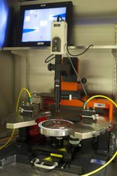
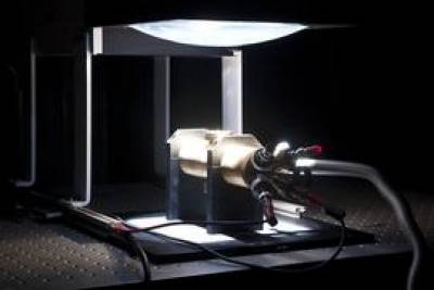
2. LCN shared facilities including clean room standard processing are accessible at the LCN-member rate. Other valuable facilities include a dual-beam focused-ion-beam (FIB), e-beam lithography, a range of scanning probe microscopes (SPMs), and an environmental SEM. The wide range of lithographic techniques available (Optical, E-beam and FIB) is especially valuable for fabrication of electrical contacts to conducting or semiconducting nanostructures.
B. Photophysical characterization & high-resolution optical patterning: Near-field & far-field studies
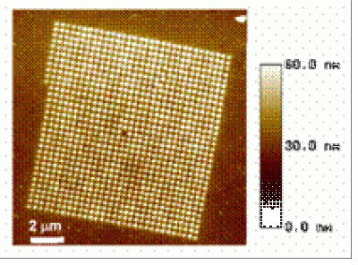
1. Scanning near-field optical microscopy (SNOM) and lithography (SNOL) are scanning probe techniques which allow effective detection and control of electromagnetic fields (from IR to UV) below the diffraction barrier (~ l/2 in air), that is in the so-called "Near-Field". For solid-state physics and organic semiconductors this provides a unique opportunity for investigating, optically, mesoscopic phenomena which occur in homogeneous and heterogeneous structures (e.g. polymer blends). The SNOM is also a marvellous tool for studying and controlling the effect of topological and energetic disorder. We operate a home-built instrument with sub-100 nm lateral resolution combining high-resolution scanning stages (range 200x200x20 μm, in XYZ directions, with positioning accuracy of 1, 1, and 0.1 nm respectively) with large travel-range stages (2.5 cm range and resolution of 100 nm, both X and Y directions), so as to be able to navigate on substrates with large dimensions, such as those that are likely to be technologically interesting. We have used this near-field microscope for both microscopy[1-5] and high-resolution lithography[6-8] (see figure below, reporting a quasi-periodic 2D pattern of PPV with an intentional defect). Available excitations sources are both in the visible (Ar-ion laser, diode lasers both CW and pulsed) and in the UV (325 nm He-CD/multi-line UV lines of the Ar-ion).
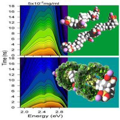
2. Far-field optical probes available include the possibility of measuring photoluminescence (PL), PL efficiency, and electroluminescence (EL) characterisation of LEDs. We also have a UV-vis-NIR absorption spectrophotometer with sample temperature control (Agilent) and a commercial Time-Correlated Single Photon Counting spectrometer (Edimburgh Instruments) to study time-resolved emission in the ns regime.
C. Characterisation of charge injection in metal/organic semiconductor/metal structures
1. Electroabsorption experiments measure the variation of the absorption response of a semiconducting material induced by the application of an electric field. For this reason they can probe both the intrinsic properties of the semiconductors (e.g. details of the energy structure), and also the electric fields present in the devices. These measurements thus constitute a powerful, non-invasive probe of devices in which an active organic semiconductor is sandwiched in between two electrodes. The beauty of the technique is that it is applicable to finished devices. In previous work we have shown the possibility to measure the variation of the barrier height (for electron or hole injection) when altering either anode or cathode (see figure above for the anode case), in connection with the development of both high and low work function electrodes[9-11].
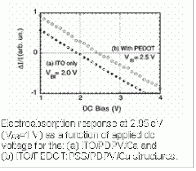
2. Electrode optimisation, achieved though electroabsorption measurements of the variation of the barrier to electron (hole) injection when altering one of the electrodes, is likely to play a primary role in the development of any organic semiconductors based optoelectronic device, both for large area applications and at the nanoscale. Characterisation of the variation of the barrier height upon switching in either the contacts or the semiconductors should be of fundamental importance for both a good understanding and a fruitful exploitation of the devices intrinsic potential. We also have the expertise and instrumentation to complement the electroabsorption results by characterising the "open electrode surfaces" via Kelvin-probe (KP) measurements. Comparison between electroabsorption and KP measurements provides information regarding the spontaneous or intentional formation/incorporation of dipole layers at the electrodes interfaces.
3. Device ageing studies can be done by combining electroabsorption experiments (to probe variation in electronic structure of the interfaces, via the built-in voltage) with purely optical probing of the materials, so as to be able to distinguish electrodes ageing from degradation or modification of the active material.
D. References
1. R. Stevenson, et al., Appl. Phys. Lett. 79, 833-835 (2001)
2. R. Riehn, et al., MRS Proc. 708, BB3.17-20 (2002)
3. G. Latini, et al., Appl. Phys. Lett. 86, 011102 (2005)
4. P. Gucciardi et al., Appl. Phys. Lett. 86, 203109 (2005)
5. R. Riehn, et al., Adv. Funct. Mat. (Submitted)
6. R. Riehn, et al., Appl. Phys. Lett. 82, 526-528 (2003)
7. F. Cacialli, et al., Ultramicroscopy 100, 449-455 (2004)
8. R. Riehn and F. Cacialli, Journal of Optics a-Pure and Applied Optics 7, S207-S212 (2005)
9. T.M. Brown, et al., Appl. Phys. Lett. 75, 1679-1681 (1999)
10. T.M. Brown, et al., J. Appl. Phys. 93, 6159-6172 (2003)
11. T.M. Brown, et al., Appl. Phys. Lett. 79, 174-176 (2001)
E. Detailed list of primary experimental equipment
1. Home-built SNOM. The instrument has been designed with nanotechnology applications in mind and includes a combination of a high-resolution scanning head (travel range of 200x200x20 µm xyz range with 1,1,0.1 nm precision respectively) and of a lower resolution long-travel range scanning stages (2.5 cm travel in both x and y direction) to allow processing and imaging of large samples, as well as to ease the process of locating of certain predefined features on the substrates of interest (e.g. electrodes or nanoelectrodes). The versatility of the instrument also lies in the "open" architecture that leaves a considerable amount of available space below the sample holder (that is optically transparent) for both transmission and reflection experiments. The microscope can be enclosed in a nitrogen-filled glove-box for processing/observation of the materials in an anaerobic, dry environment. The optics includes 2 remotely operated CCD cameras for the alignment operations. The lasers are: (i) an Ar-ion laser (Stabilite 2017 from Spectra Physics) with UV option, (351/363.8 nm) in addition to the visible (457.9 to 514 nm), and (ii) a He-Cd Laser (325) nm. A TCSPC system with ps pulsed laser (400 nm) is currently being added to the set-up.
2. Facilities for spin-coating and other processing/characterisation of polymeric semiconductors, and of the suitable substrates (fume hood, glove-box integrated with a thermal evaporator and spin-coater, oxygen plasma oven for the treatment of the substrates, surface profilometer, optical microscopes, microbalances).
3. Fully equipped clean room in the department of EE (fully accessible by FC as a member of the LCN).
4. LCN facilities. The main pieces of capital equipment available within the LCN are:
 Close
Close

