The small entropy of mixing of polymers leads, naturally, to self-organisation and phase-separation of heterogeneous polymer blends processed from the same solution, with domains size from few nm upwards. When suitable semiconductors are selected, these are nanostructures with significant electronic functionality. For example, in photovoltaic diodes, important parameters are the energy level offsets between the highest occupied molecular orbitals (HOMO) and the lowest unoccupied molecular orbitals (LUMO) of the different polymers. When such offsets are large enough exciton dissociation at the polymer interface is energetically favourable. Optimum balance between phase-separation on a fine scale (~10 nm) to achieve a large charge transfer yield, and phase segregation on a longer length scale to allow efficient charge percolation to the appropriate electrode, and avoid efficient geminate recombination, must also be achieved to ensure efficient photovoltaic conversion.
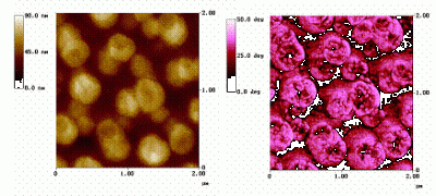
The AFM is an important tool to study the surface morphology associated with phase separation, as it provides very high resolution with minimum perturbation of the samples, leading to significant insight into the rich surface structure of these phase separated blends (see the topography (left panel) and the phase (right panel) images shown).

AFM images of a phase separated blend of a binary blend of conjugated polymers from the polyfluorene family. Left panel shows topography, right panel shows phase
The project will study blends of conjugated polymers for optoelectronic applications and will focus in particular on the mechanisms of formation and evolution of phase-separated nanostructures upon spin-coating of a multi- solution.
The final aim is to achieve control over the nanostructures formation and evolution, by a deeper understanding of the crucial parameters influencing such phenomena.
 Close
Close

