Telecommunications wavelength quantum dot laser grown on silicon substrate
13 June 2011
A new generation of high speed, silicon-based information technology has been brought a step closer by researchers in the Department of Electronic and Electrical Engineering at UCL and the London Centre for Nanotechnology.

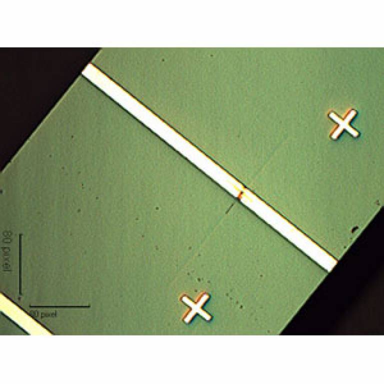
The team's research, published in Nature Photonics journal, provides the first demonstration of an electrically driven, quantum dot laser grown directly on a silicon substrate (Si) with a wavelength (1300-nm) suitable for use in telecommunications.
Silicon is the most widely used material for the fabrication of active devices in electronics. However, the nature of its atomic structure makes it extremely hard to realise an efficient light source in this material.
As the speed and complexity of silicon electronics increases, it is becoming harder to interconnect large information processing systems using conventional copper electrical interconnects. For this reason the field of silicon photonics (the development of optical interconnects for use with silicon electronics) is becoming increasingly important.
The ideal light source for silicon photonics would be a semiconductor laser, for high efficiency, direct interfacing with silicon drive electronics and high-speed data modulation capability. To date, the most promising approach to a light source for silicon photonics has been the use of wafer bonding to join compound semiconductor laser materials from which lasers can be made to a silicon substrate.
Direct growth of compound semiconductor laser material on silicon would be an attractive route to full integration for silicon photonics. However, the large differences in crystal lattice constant between silicon and compound semiconductors cause dislocations in the crystal structure that result in low efficiency and short operating lifetime for semiconductor lasers.
The UCL group has overcome these difficulties by developing special layers which prevent these dislocations from reaching the laser layer together with a quantum dot laser gain layer. This has enabled them to demonstrate an electrically pumped 1,300 nm wavelength laser by direct epitaxial growth on silicon. In a recent paper in Optics Express (Vol. 19 Issue 12, pp.11381-11386 (2011)) they report an optical output power of over 15 mW per facet at room temperature.
In related work the group, working with device fabrication colleagues at the EPSRC National Centre for III-V Technologies, have demonstrated the first quantum dot laser on a germanium (Ge) substrate by direct epitaxial growth. The laser, reported in Nature Photonics , (DOI: 10.1038/NPHOTON.2011.120, 12 June 2011) is capable of continuous operation at temperatures up to 70 deg. C and has a continuous output power of over 25 mW per facet.
Leader of the epitaxy research that enabled the creation of these lasers and Royal Society University Research Fellow in the UCL Department of Electronic and Electrical Engineering, Dr Huiyun Liu, said: "The use of the quantum dot gain layer offers improved tolerance to residual dislocations relative to conventional quantum well structures. Our work on germanium should also permit practical lasers to be created on the Si/Ge substrates that are an important part of the roadmap for future silicon technology."
Head of the Photonics Group in the UCL Department of Electronic and Electrical Engineering, Principal Investigator in the London Centre for Nanotechnology and Director of the EPSRC Centre for Doctoral Training in Photonic Systems Development, Professor Alwyn Seeds, said: "The techniques that we have developed permit us to realise the Holy Grail of silicon photonics - an efficient, electrically pumped, semiconductor laser integrated on a silicon substrate. Our future work will be aimed at combining these lasers with waveguides and drive electronics leading to a comprehensive technology for the integration of photonics with silicon electronics."
 Close
Close

